Traditionally, Metal ECO involves traversing between the backend database and frontend netlist during ECO. Implementing a straightforward AND gate insertion fix demands an exhaustive search for spare resources within the backend database. GOF integrates resource exploration and logic correction into a unified platform. The subsequent use case demonstrates importing the physical database into GOF and identifying suitable spare gates to rectify an AND logic insertion.
The logic alteration is straightforward: appending an AND gate to one output signal. However, the enable signal for the AND gate might require some distance. Spare buffers could be necessary to drive the enable signal.
Load in netlist and physical files by the command
../bin/gof -lib tm40.lib -def tser_post.def -lef tm_hvt.lef tser_post.v
When GofViewer Netlist browser window is up, find the related net and click 'New Schematic' button.
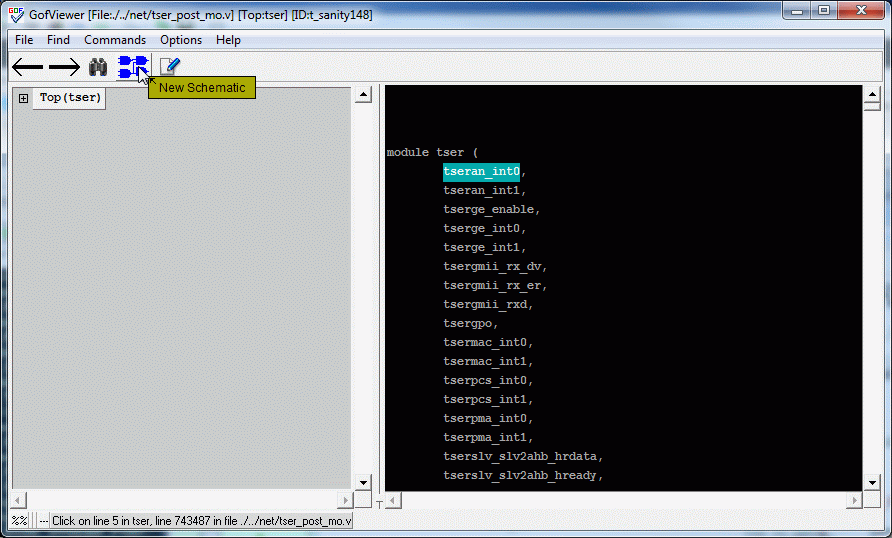
Figure 1. Load GUI database and bring up schematic
Starting from the port, 'tseran_int0', use mouse-middle-button to trace the gates. Load the enable signal 'rx_mode' to the schematic as well and trace to make a proper circuit.
The logic change is essentially, "tseran_int0 = original_tseran_int0 & rx_mode"
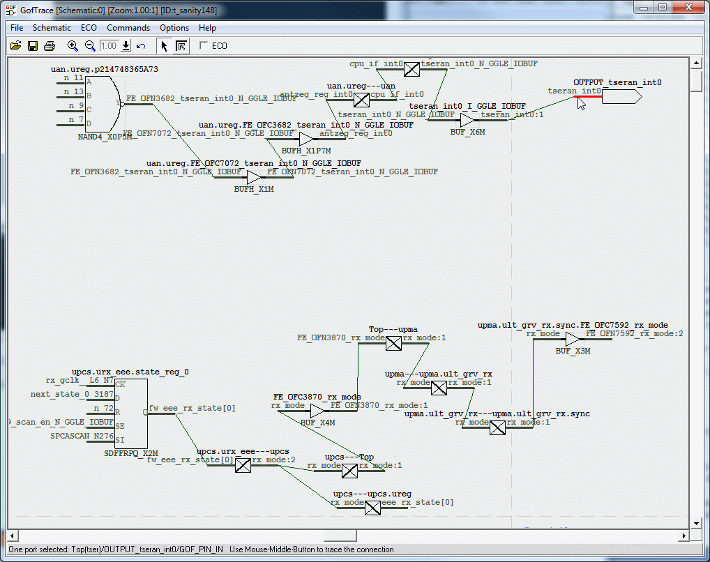
Figure 2. Load related gates and signals
Select the circuit under fix, right click mouse to select 'Copy Selected to' -> 'Layout New'
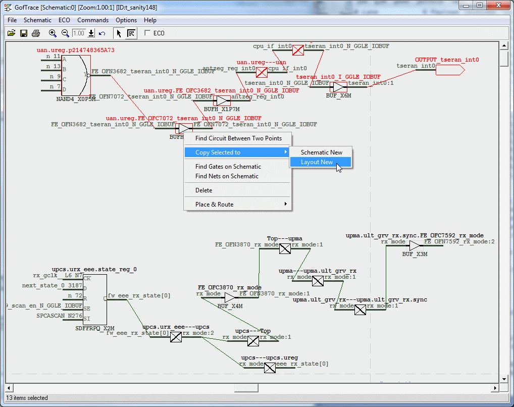
Figure 3. Send circuit to LayoutViewer
The circuit is shown on LayoutViewer as lines and arrows.
Click to select another color when the first circuit is shown on LayoutViewer. So the new circuit view will be displayed in different color.
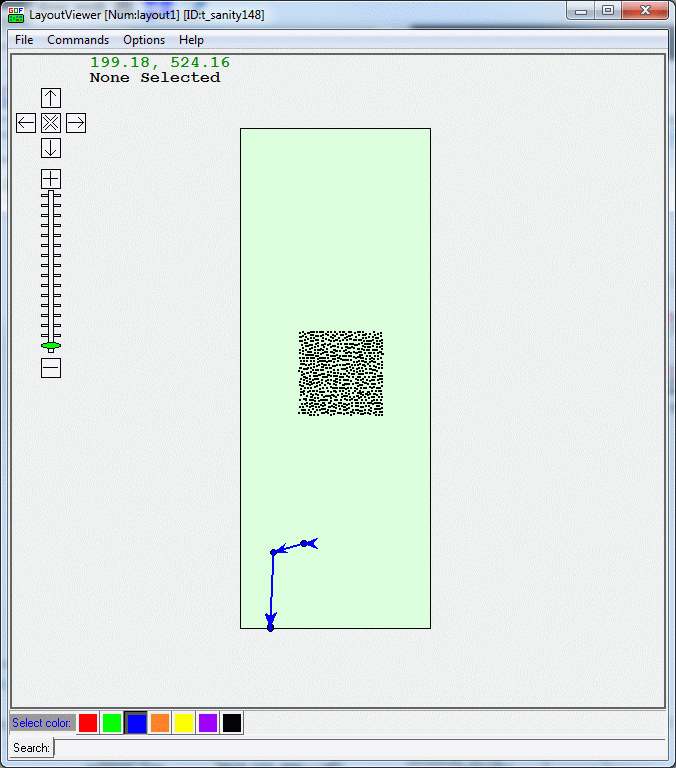
Figure 4. LayoutViewer 1
Select the enable logic circuit and send to the same LayoutViewer Index
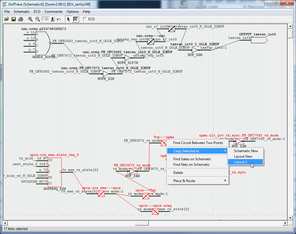
Figure 5. Send enable logic to LayoutViewer
Now two circuits are on one LayoutViewer. Find the closest part of them, spare gates will be found in that part.
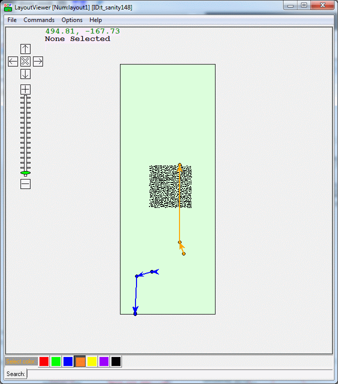
Figure 6. Two related circuits shown on the same LayoutViewer
Zoom in to closest part between two circuits. Proper spare gates will be found in this area.
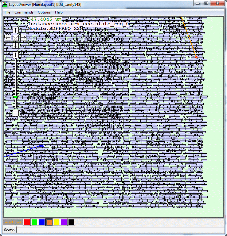
Figure 7. Zoom-in to the right place
Select color 'green'.
Type 'mySpare*/*spr_gate*' in the bottom Search entry and high light all spare gates on the LayoutViewer.
Spare gates have type NAND NOR MUX INV, so AND gate has to be NAND+INV. A buffer is needed to drive 'rx_mode' signal from the circuit in orange. The buffer can be created from two back to back inverts.
So total 3 inverters and one NAND gate are needed.
Find NAND and INV gate close to the circuit in blue. 'mySpare_tserspr_23.NAND2_X4M_spr_gate326' and 'mySpare_tserspr_16.INV_X9M_spr_gate235'
Find big driver INV close to orange circuit, 'mySpare_tserspr_32.INV_X9M_spr_gate458'. Find another INV in between blue and orange circuits, 'mySpare_tserspr_23.INV_X9M_spr_gate333'
These two inverts are connected back to back to create a buffer.
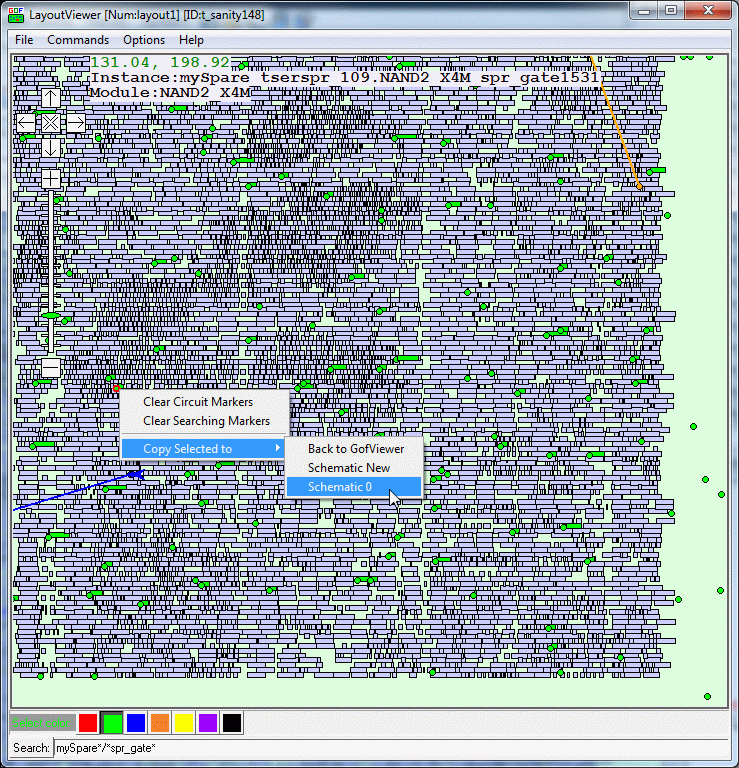
Figure 8. Spare gates process on LayoutViewer
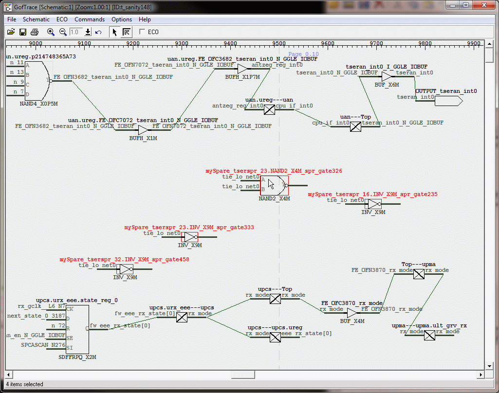
Figure 9. Spare gates on schematic
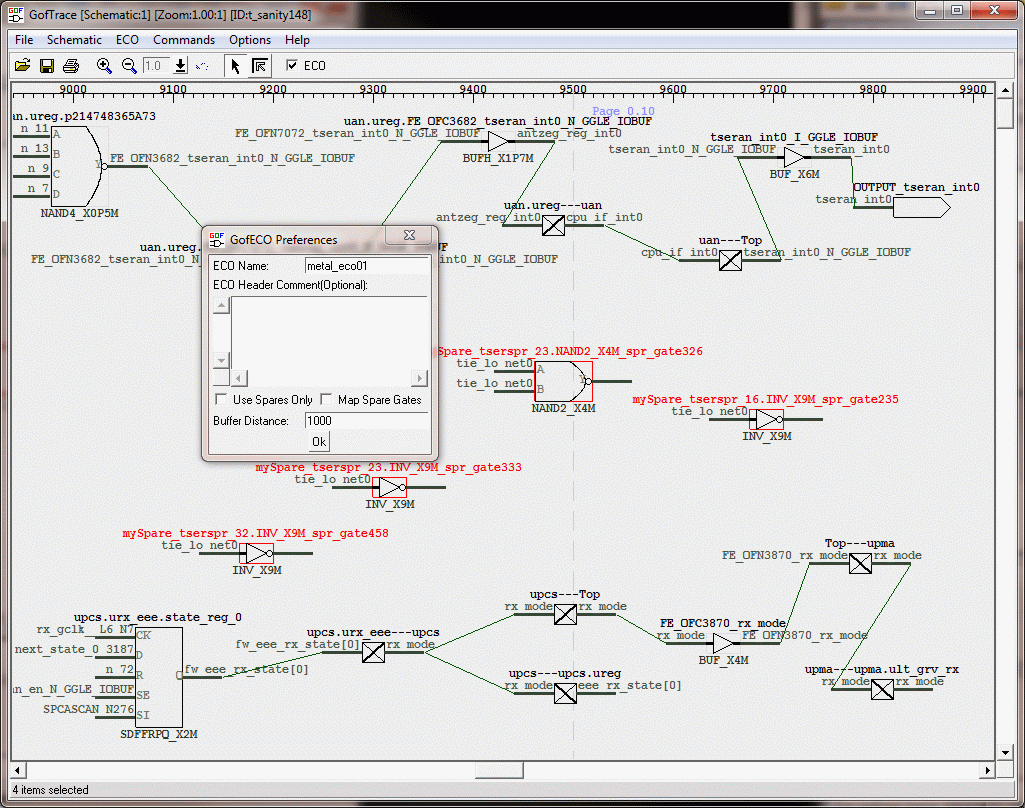
Figure 10. Enable ECO
Trace inputs to spare gates and delete the connections.
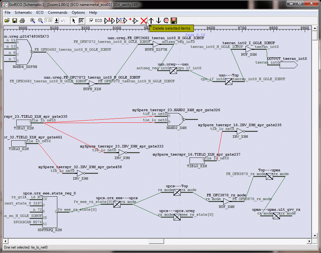
Figure 11. Delete spare gates inputs
The best place to insert AND gate is NAND4 output which is closest to the enable signal 'rx_mode'
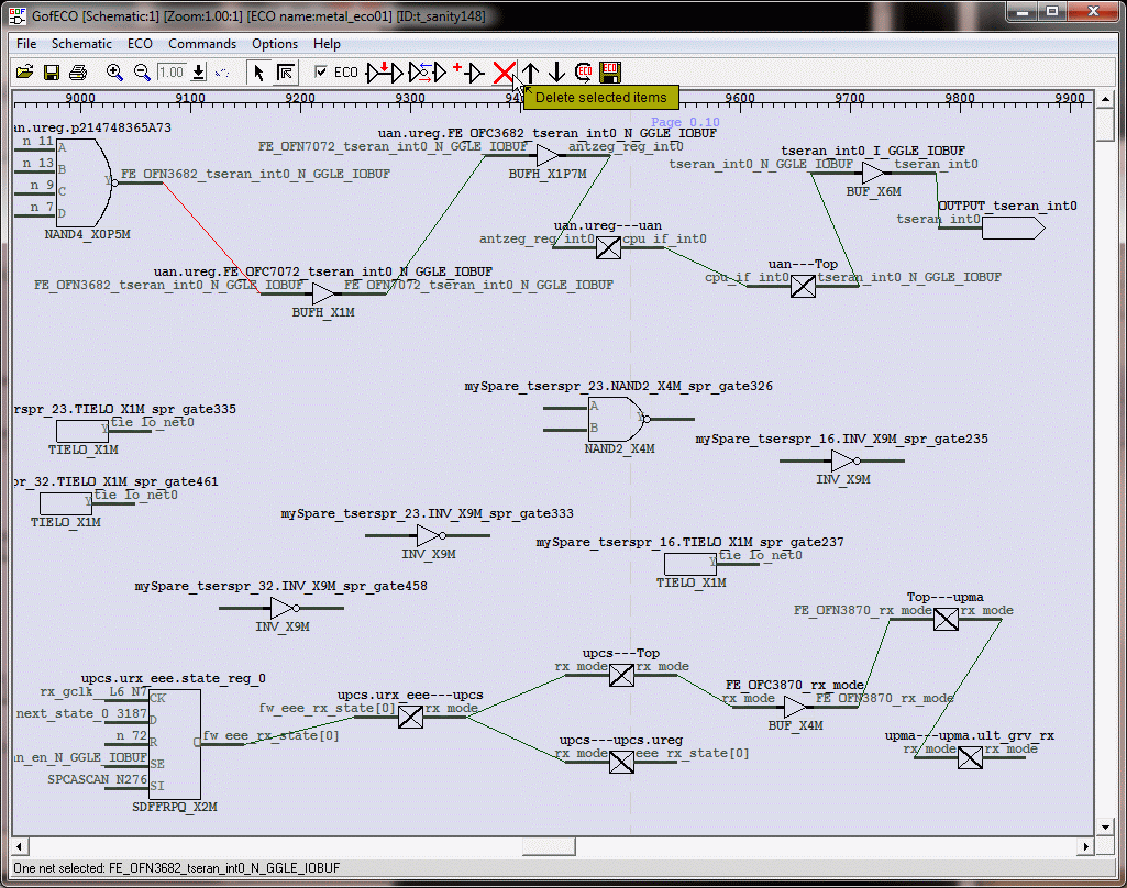
Figure 12. Disconnect ECO spot
Press mouse-middle-button on a spare input pin, don't release the button and move the button to the other gate's output pin it should connect to. Then release the button.
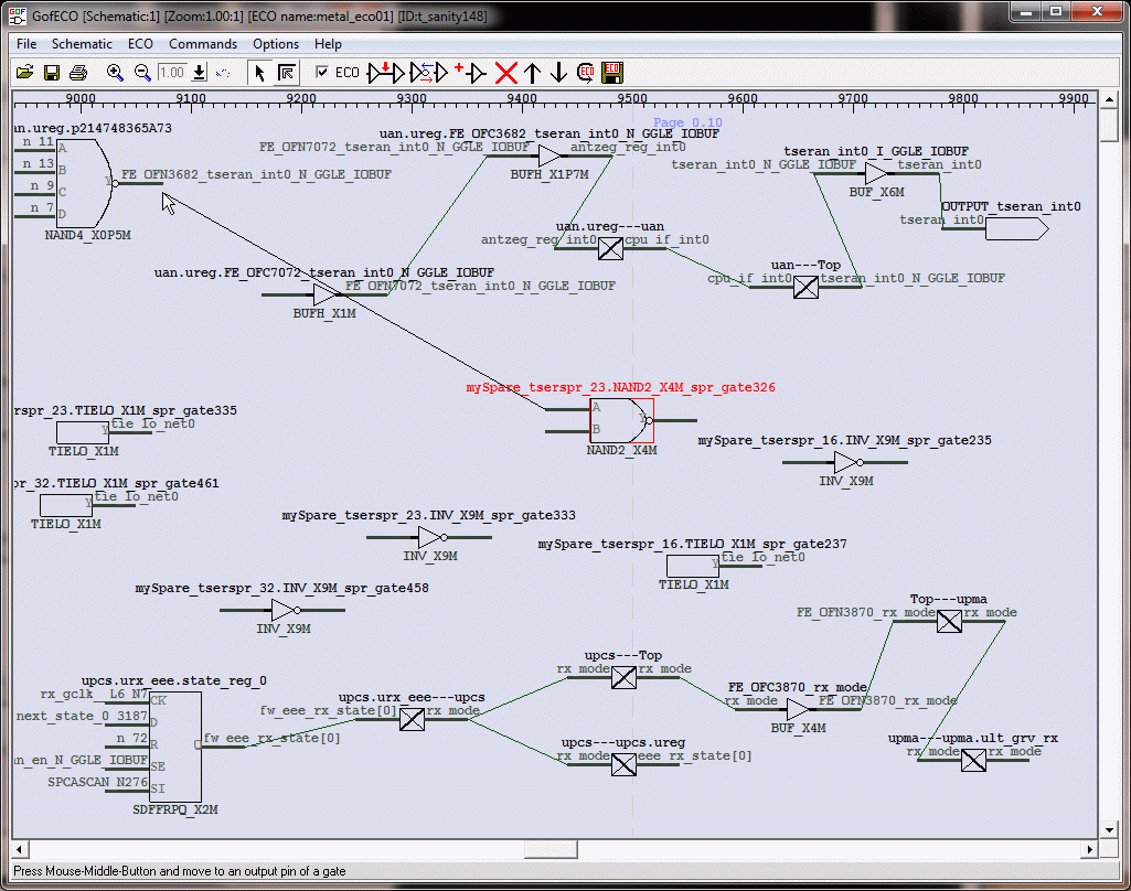
Figure 13. Wire connecting
One connection is done and ports are automatically added to bridge up the hierarchies.
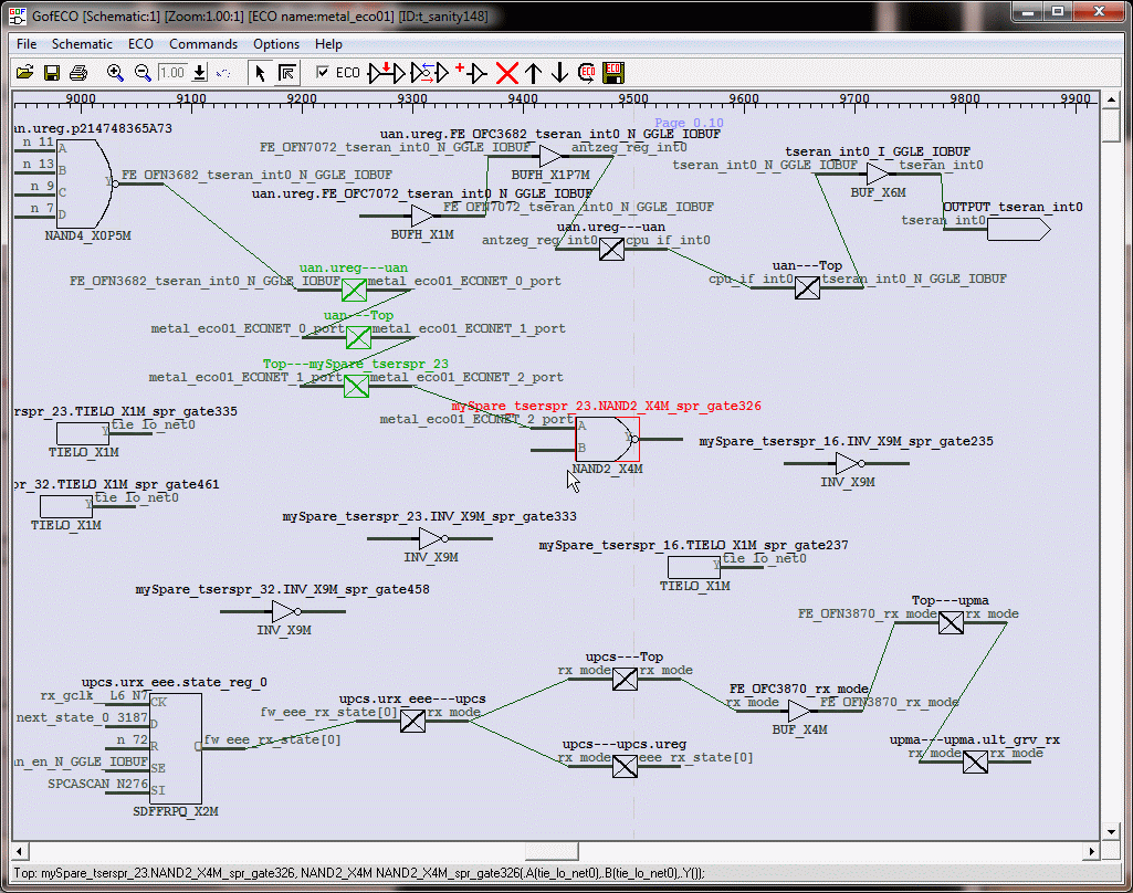
Figure 14. Connection done
Save the ECO in verilog mode, 'tser_eco.v'
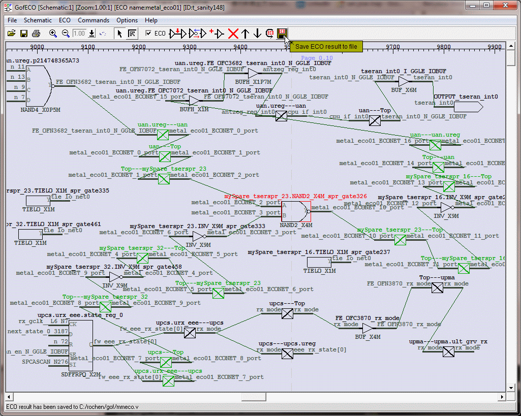
Figure 15. ECO complete schematic
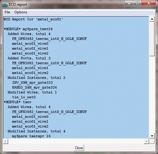
Figure 16. ECO report
Load tser_eco.v and related physical files.
../bin/gof -lib tm40.lib -def tser_post.def -lef tm_hvt.lef tser_eco.v
Draw the related circuit and send to a new LayoutViewer.
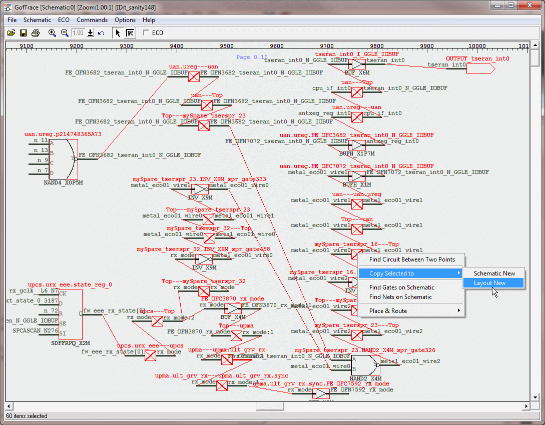
Figure 17. Draw complete circuit
Compare with figure 6, it's easy to see the spare gates used and connections are in the right location.
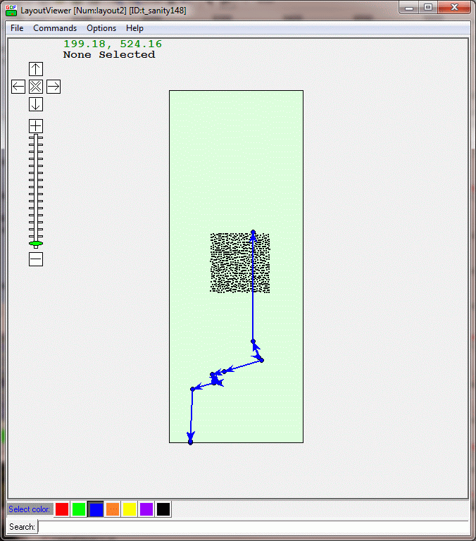
Figure 18. ECO verified on LayoutViewer