Power gating implementation and verification
Power gating is to shut off the power of a cluster of gates on the die to save leakage current. With respect to total power consumption, leakage power has increased to to over 50 percent in 65-nm designs, power gating methodology is adopted by more and more design companies. The basic method is shutting the external power but it's slow. The more comprehensive way is to make power controllable inside the chip which is much fast to power on off. Practically the power is controlled by PMOS/NMOS transistors. And NMOS is picked against PMOS since it has fast response time and driver capability than PMOS. And the selection of NMOS makes GND controllable not VDD.
2. What should be done to the power gated partitions?
P&R side has to implement the NMOS control mechanism and other power rails layout. This topic is focus on netlist side.
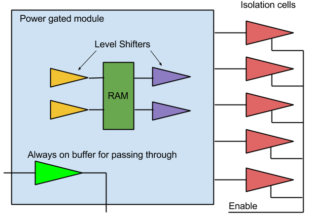
The power gated partition should have isolation logic for the output ports to other non power gated partitions. The isolation logic is basically an AND gate. Every output port from power gated partition to non power gated partition should have an AND gate to isolate the "floating" wire. The "floating" wire is charging slowly to the value of VDD when the partition is gated off. And the "floating" wire has high driver impedance.
The power gated partition should have some Always On Logic which can't be shut off by the NMOS, that is to say, their GND is not controlled by NMOS, but real power ground instead. The feeding through paths and the NMOS control signal have to use Always On Logic in order to retain the right value in power gated mode. If the isolating AND gate is in power gate partition, it has to be always on too. These Always On Logic requires a new set of library with different naming for easy detection in verification stage.
Power nets, GND VDD or other gated GND, should be explicitly present in the netlist in order to verify the power implementation.
3. How to verify the power implementation?
The isolation AND gates and the always on logic should be checked as implemented correctly. If the isolation AND gates are inserted after synthesis, the enable input of the AND gate is set to disabled value in Logic Equivalence Check. So these AND gates are not covered in formal run in this case. But even the isolation AND gates already exist in RTL, there is still a need to check they are correctly implemented in the netlists.
The common issues for power gating flow in timing closure stage includes:
Case 1 can't be fixed by the EDA tools themselves, since you can't ask all EDA tools to recognize the Always On Logic paths. So the post-processing script becomes a practical choice.
GofCall scripts can be used in verifying and fixing the issues.
For the feeding through paths to be always on: